
In modern life, each and every one of us is covered by radio signals (WIFI, Bluetooth, mobile phones, communication base stations, walkie talkies, etc.) every day. In electronic instruments and equipment, as one of the important core chip components, the instrument amplifier can extract weaker differential signals from strong common mode noise and interference due to its inherent common mode suppression ability under the interference of these RF signals. This is especially evident in situations where the signal transmission line is long and the signal strength is low. This potential issue is often overlooked, which is the RF rectification problem present in instrument amplifiers. When there is strong radio frequency interference, the integrated circuit may rectify the interference and then exhibit DC output offset error. The common mode signal at the input end of the instrument amplifier is usually attenuated by its common mode suppression performance. Unfortunately, RF rectification still occurs because even the best instrument amplifiers cannot effectively suppress common mode noise when the signal frequency is above 20 kHz. The input stage of an amplifier may rectify strong RF signals and then exhibit DC offset errors. Once rectified, the low-pass filter at the output of the instrument amplifier will not be able to eliminate this error. If radio frequency interference is intermittent, it can lead to measurement errors that cannot be detected. The domestically produced and high-precision analog operational amplifier chip XL620 introduced in this article can reduce the occurrence of such problems and help improve the performance of various instruments and equipment!
The high-performance instrument amplifier XL620 independently developed by Xinluda Information Technology (Xiamen) Co., Ltd. is a low-cost and high-precision amplifier that can be set with a gain of 1-10000 with just one external resistor. The input stage of XL620 adopts Super ß eta processing, so it can achieve a maximum low input bias current of 1nA, with the characteristics and advantages of low offset voltage (maximum 50 µ V) and low offset drift (maximum 0.6 µ V/° C)! Very suitable for products that require high-precision analog devices, such as data acquisition systems, industrial process control, medical equipment, electronic scales, sensor interfaces, and so on.
1. Design a practical RF interference filter using XL620
The most practical solution to this problem is to use a differential low-pass filter before the instrument amplifier to attenuate the RF signal. This filter has three functions: to eliminate as much RF energy as possible in the input line; Balance the AC signal between each line and the ground (shared); And maintain a sufficiently high input impedance throughout the entire measurement bandwidth to avoid increasing the load on the signal source.
The following diagram shows a practical RF interference suppression circuit constructed using XL620
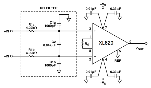
The instrument amplifier XL620 has a high noise level (12 nVHz) and a low bandwidth. When using the values shown in the figure, the -3 dB bandwidth of the circuit is approximately 400Hz; By reducing the resistance values of R1 and R2 to 2.2 k Ω, the bandwidth can be increased to 760 Hz. It should be noted that increasing bandwidth comes at a cost, requiring the impedance load driven by the circuit in front of the instrument amplifier to be lower, which will to some extent reduce the input overload protection performance.
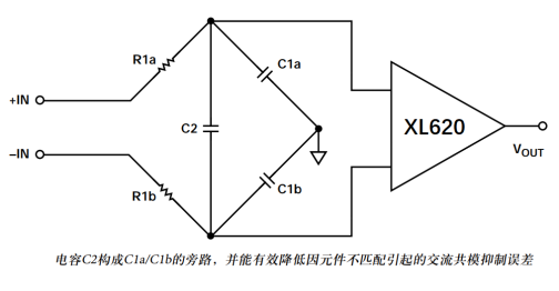
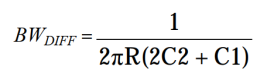
The above diagram is a simplified representation of the anti RF interference circuit. As can be seen from the figure, the filter forms a bridging circuit, with its output spanning between the input pins of the instrument amplifier. Given this connection method, any mismatch between the time constants C1a/R1a and C1b/R1b can lead to bridge circuit imbalance, thereby reducing the high-frequency common mode suppression performance. Therefore, the resistors R1a and R1b, as well as the capacitors C1a and C1b, should always be equal. As shown in the figure, C2 is connected across the output end of the bridge, so that C2 is actually in parallel with the series combination composed of C1a and C1b. After this connection, C2 can effectively reduce any AC common mode suppression error caused by mismatch. For example, if C2 is 10 times larger than C1, this connection method will reduce the common mode suppression error caused by C1a/C1b mismatch to one twentieth of the original. It should be noted that this filter does not affect DC common mode suppression. RF interference filters have two different bandwidths: differential bandwidth and common mode bandwidth. Differential bandwidth is defined as the frequency response of a filter when inputting differential signals at two input terminals (i.e.+IN and - IN) of a circuit. The RC time constant is determined by the sum of two equivalent input resistances (i.e. R1a, R1b) and the differential capacitance (i.e. C2 in series and parallel with C1a and C1b).
The -3dB differential bandwidth of this filter is equal to:
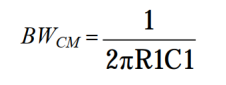
The common mode bandwidth is defined as the bandwidth of the common mode RF signal between two interconnected inputs and ground. It must be noted that C2 does not affect the bandwidth of the common mode RF signal, as this capacitor is connected between two input terminals (helping to maintain the same RF signal level). Therefore, the common mode bandwidth is determined by the ground parallel impedance of the two RC networks (R1a/C1a and R1b/C1b) The 3dB common mode bandwidth is equal to
Taking the application circuit of XL620 as an example, if C2=0.01 μ F, the bandwidth of the -3dB differential signal is about 1900Hz. When the gain of the circuit is 5, its measured DC offset voltage in the frequency range of 10Hz to 20MHz is less than 6 μ VRTI. Under unit gain conditions, this DC offset voltage can be ignored.
In practical applications, RF interference filters should be designed using printed circuit boards (PCBs) with both sides grounded, and all component leads should be as short as possible. Resistors R1 and R2 can be made of ordinary 1% metal film resistors. However, all three capacitors must be high Q value low loss components. Capacitors C1a and C1b must be devices with a tolerance of ± 5% to avoid reducing the common mode suppression performance of the circuit. It is recommended to choose traditional 5% silver plated mica capacitors, small mica capacitors, or high-precision ± 2% polyphenylene sulfide (PPS) thin film capacitors.